
US President Joe Biden holds up a silicon wafer in the White House during a virtual summit on the semiconductor shortage that has been dominating supply chain woes globally. (Photo by Brendan Smialowski / AFP)
Perfect circle: Micron spearheads tech breakthroughs with world’s first 232-layer NAND
It has been a bumper year, but a rollercoaster one for the global semiconductor space, and pioneering hardware manufacturer, Micron Technology Inc, has been right in the thick of it. Following record demands for its memory and storage products, Micron (not for the first time) became the first chipmaker to begin volume production of the world’s first 232-layer NAND at the company’s Singapore fabrication plant, or fab.
Tech Wire Asia took the opportunity to speak with Nagasubramaniyan (Naga) Chandrasekaran, the Senior Vice President of Technology Development at Micron, on this significant technological achievement, as well as to tour the impressive Singapore fab, including notably Micron’s gleaming FAB10N clean room and Remote Operations Centre (ROC).

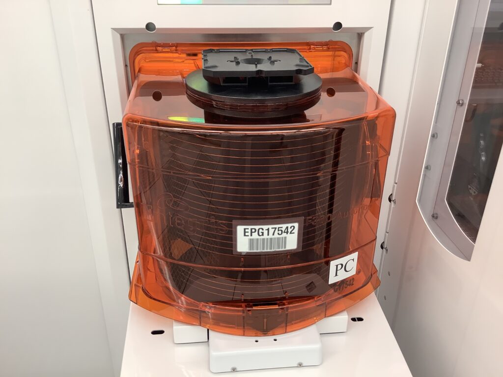
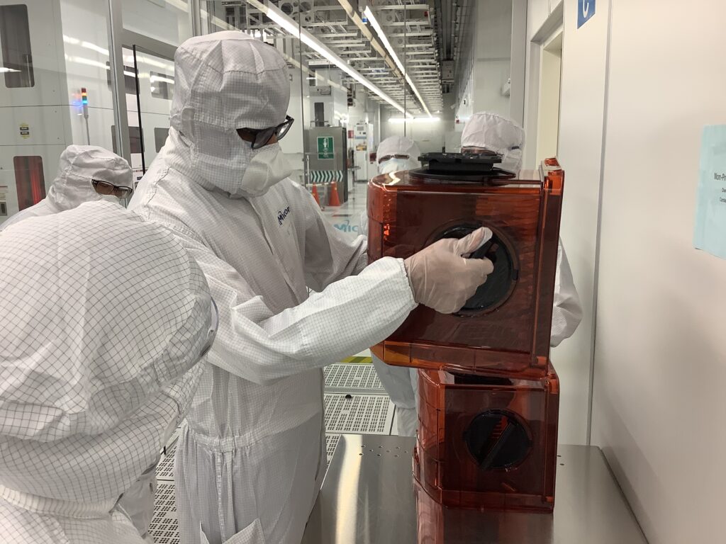
Inside Micron Singapore’s heavily automated, intelligently designed FAB10N clean room. Source: Micron Technology
For the uninitiated, NAND is a type of flash memory that relies on electric circuitry to store data, even without an external power source. Once power is detached from NAND flash memory, a metal-oxide semiconductor continues to supply an extra charge to the memory cell, storing data intact. Ever since data storage started going fully digital and requiring hardware merely to house the flash memory, NAND has become the popular choice to store large files that can be frequently uploaded and replaced – which is why MP3 players, digital cameras and USB flash drives all utilize NAND memory.
Since Micron’s initial announcement, other fabricators have revealed their own 232-layer NAND, but Micron is the first to go to production with this highest-layer NAND, wholly manufactured at the Singapore plant, which is also Micron’s NAND Center of Excellence that has been hailed by the World Economic Forum’s Global Lighthouse Network for operational excellence in smart manufacturing.
“So very proud of this one, the 232-layer, where we were the first ones to announce this. But more than the announcement, it’s in my opinion, significantly ahead by months in terms of productization, and being already running in volume here in Singapore,” enthused Naga, commenting how certain 232-layer NAND components are already being sold in the market through Micron’s crucial SSD channel, along with shipping samples to electronics customers.


This is not the first time that Micron has broken the NAND innovation mould either – Micron was also first to market with the 176-layer NAND, the pinnacle of NAND layers that was the industry benchmark at the time. “And I tell our teams also that it’s not just a one-shot wonder, right, like when the 176-layer came out, Micron announced first, and it shocked the industry,” Naga confirmed.
“And then now with 232, it’s two in a row [industry firsts] that we are able to get. And it’s all because of the innovation that’s happening with the Micron team members, and also the role that Singapore is playing in our NAND portfolio.”
Micron’s Singapore facilities were first established more than two decades ago when the semiconductor specialists acquired Texas Instruments, and today employs over 8,000 team members (Micron employees are all called team members, and the company has been repeatedly recognized as a Great Place to Work in Singapore).
Naga himself has been with Micron since 2001, and has been coming to the Singapore operation since 2003. As an industrial trailblazer Micron has been heavily involved in many innovations from storage hardware to smart manufacturing breakthroughs to running one of the most automated and precise Remote Operations Centers in the world – but Naga counts having once again shipped a first-of-its-kind NAND deployment, fully researched and manufactured out of the Singapore, among his proudest achievements.
Silicon wafers that used to be assembled painstakingly by hand, are now largely automated. Source: Micron Technology
“I’m very proud of the innovation that happens across the semiconductor industry – of course Micron, but across the semiconductor industry – a lot of the fundamental mechanisms we understand,” he noted.
“But there’s five years of R&D behind getting one of these products out into the market, right, five-plus years. And that’s the five-plus years where fundamentals, modelling, with some empirical work that we are doing on the silicon, all of those together is how you get to these pieces,” summarized Naga, before adding, “Of course, it’s all people eventually. People have to come up with the innovations and ideas.”
How big of a breakthrough is the 232-layer NAND in actual fact? It all lies in Micron’s layers and six-plane architecture. When it comes to memory hardware, its about maximizing the space on the board to incrementally optimize efficiencies. Built upon industry-leading pioneering technologies in its 176-layer NAND, not only does the 232-layer possess the highest layer count, it also spits out the most bits-per-millimeters-squared and generates the fastest input/output read speeds in its class.

Naga Chandrasekaran, SVP Technology Development at Micron Technology
Naga says that with the right architecture and process changes, along with the likewise industry-first six-plane one terabit device, “we can get 200% write bandwidth improvement, and a 75% read bandwidth improvement” in contrast with the previous generation technology node.
“Us coders like to say it’s like a supermarket where you have one lane, you can consider it as one plane. But now we have increased the number of lanes, which is the sixth plane, it allows you more checkout lanes to come out,” he elaborates. “And then on top of it, now we have a higher data transfer. So more people can get through each link, we are able to put push more data back and forth through this.”
“All of this means our latency is going to be really fast, and how we can move the data around. And it’s going to give some energy efficiency as a result. So those are some pretty good numbers.” And since its physical capacity, or density, is what will determine how efficient, fast, and how much better latency will be improved, Naga went on:
“Compared to things in the market, other competitors, it’s anywhere between 35-to-100% more bits in terms of density that we are able to get. But we are doing that in a much smaller footprint. So this is 11.5 by 13.5-millimeter square package. And that’s a 28% reduction in the site size. So now we can get a lot more areal density and a much smaller size, with better performance. All of this is really getting us to the fast storage, better latency, and efficiency.”
So for devices like laptops and flagship smartphones, the memory performance output is going to be much higher, but with a smaller footprint, lower rate, and much higher density. “And that’s going with the cost reduction, the performance is actually going to give more storage for the moment. But then power is going to be lower, in terms of the total read-write energy is going to be better. And that’s going to give you better battery life.”
Not just the consumer spaces will see sizable benefits, but in commercial applications from on-premises storage to the automotive industry to software applications. “Now, because of the higher density and the form factor for the same footprint, we can put more than [one terabit in a NAND package]. As a result, the data center applications for AI (artificial intelligence) or ML (machine learning) can have a lot more storage. We have more storage with better data transfer rate. You can get to much more real-time data and much better storage.”
The Clean Room & Remote Operations Center feature state of the art RPA, AI, intelligently optimized with data science. Source: Micron Technology
Micron has been accelerating performance efficiencies in its NAND and other products — by accelerating efficiencies in its R&D, operational processes, and its smart manufacturing processes with a combination of intelligent data analytics and equipment enhancements that leverage cutting-edge robotic process automation and intelligent machinery that leverage AI to predict space optimization. Its FAB10N clean room, where the ultra-sensitive wafers are assembled with precision and speed, is one of the cleanest in the world.
“It’s not just the technology, but all the AI aspects that we are doing here. That’s helping us to improve the yield aspects faster, we don’t want to just run wafers without improving the yield,” elaborates Naga. “So we are doing a lot of machine learning, data analytics, using data science to actually improve our yield, improve our equipment productivity, so that we can drive better operational efficiency in the factory.”
This sort of full-circle dependency on harnessing high-end technology to build more sophisticated technology with precision, speed, and efficiency in mind, is why Micron Singapore was recognized by the World Economic Forum as a Global Lighthouse for Industry 4.0 operational excellence.
“In fact, Singapore factory is the first semiconductor fab to be recognized for Industry 4.0 – we put a lot of effort into AI/ML. That’s why I say memory and storage are enabling AI/ML [innovation],” emphasizes Naga. “Without it, we cannot get real-time data analytics and all the edge applications that we are running.
“But then the circle is completed when we use the same AI/ML solutions to improve our memory technology – performance, yield, cost, everything. So it really has come full circle.”
As perfect a circle as one of Micron’s precision cut wafers, some might say.
READ MORE
- The criticality of endpoint management in cybersecurity and operations
- Ethical AI: The renewed importance of safeguarding data and customer privacy in Generative AI applications
- How Japan balances AI-driven opportunities with cybersecurity needs
- Deploying SASE: Benchmarking your approach
- Insurance everywhere all at once: the digital transformation of the APAC insurance industry