Nvidia’s AI strategy in semiconductor manufacturing. (Source – Nvidia)
How Nvidia is using AI chatbots to craft smarter chips
- Nvidia is revolutionizing chip design by integrating AI and chatbots.
- Nvidia’s use of AI and chatbots is reshaping chip manufacturing, pioneering smarter and more efficient engineering.
- How long will it be before AI routinely outperforms humans in chip design?
Nvidia is spearheading the integration of AI into its chip design processes by incorporating chatbots, a strategy reflecting the larger tech industry’s shift towards more AI-centric solutions. This initiative shows Nvidia’s commitment to AI (and to staying ahead of the pack), and represents a pivotal change in how AI can simplify and streamline complex engineering tasks.
By introducing chatbots into its chip design framework, Nvidia aims to refine its design methodologies and establish a new precedent in the application of AI in technology development. The company is betting that using AI to design smarter chips will significantly influence the future of AI-assisted engineering.
Nvidia’s recent research is focused on using chatbots capable of generating conversational, human-like responses in semiconductor design. This research illuminates how companies in niche sectors can tailor large language models (LLMs) to their own datasets, creating specialized assistants that enhance operational efficiency.


The AI revolution in semiconductor design
Semiconductor design is an extraordinarily complex endeavor. The intricate architecture of state-of-the-art chips like Nvidia’s H100 Tensor Core GPU can be compared to a densely populated city under a microscope, consisting of billions of transistors, each a fraction of the width of a human hair.
The design of modern microchips, involving the strategic placement of tens of billions of transistors on a silicon wafer, is among the most challenging tasks in the tech industry. To construct such a digital metropolis, diverse engineering teams often collaborate for up to two years. These teams are responsible for various tasks ranging from the overall architectural blueprint, to crafting microscopic circuits, and thoroughly testing their functionalities. Each of these roles demands specialized methods, software, and computer languages.
Nvidia’s chips, recognized for their complexity, are pivotal in powering advanced technologies, including AI systems like ChatGPT. This complexity necessitates continual innovation and precision in design and execution.
The study conducted by Nvidia discovered that incorporating extensive, specific internal data enabled even basic chatbots to outperform their advanced counterparts in accuracy. This approach not only optimizes performance but also helps manage and control system costs.
How AI can benefit engineering

Nvidia’s using AI to design new chips.
One of the standout features demonstrated by Nvidia is the use of AI in generating code. Bill Dally, Nvidia’s chief scientist, pointed out that engineers often spend considerable time identifying and diagnosing faults in chip components. AI systems can alleviate this burden by rapidly writing code scripts and facilitating testing.
Mark Ren, an Nvidia research director, believes that in the future, large language models will be instrumental across all facets of semiconductor design.
“This is an important first step in applying LLMs to the complex work of designing semiconductors,” said Dally. He emphasized the feasibility of highly specialized sectors using their own data to train effective AI models.


Nvidia’s engineers have created ChipNeMo, a bespoke LLM tailored for their specific design needs, trained on the company’s confidential data. ChipNeMo is a pioneering project investigating the potential applications of LLMs in industrial chip design.
The team opted for unique domain adaptation techniques rather than using generic LLMs. This included deploying custom tokenizers and domain-specific training to enhance the model’s performance in specific applications like engineering assistance, script generation, and bug analysis.
These techniques have already shown promising results, significantly improving the model’s efficacy and suggesting possible reductions in model size while maintaining or enhancing performance in various design tasks.
Nevertheless, a noticeable disparity remains between the current achievements and the ideal outcomes. Nvidia’s team is confident that further exploring domain-adapted LLMs could help bridge this gap, leading to even more sophisticated and efficient chip design methodologies.
Looking ahead, Nvidia engineers want to apply generative AI throughout the chip design process, potentially unlocking substantial improvements in productivity and innovation. With a career spanning over two decades in electronic design automation (EDA), Ren foresees this AI integration as a game-changer in the semiconductor industry.
Among the innovations, the bug maintenance tool has drawn significant acclaim. This tool, which automates the upkeep of known bug descriptions, has proved invaluable in streamlining the debugging process.
A prototype chatbot designed to respond to questions regarding GPU architecture and design showed potential in early tests, letting engineers access pertinent technical documents rapidly. In development, a code generator already produces short snippets of software in two languages used by chip designers. This generator is set to be integrated into current design tools, offering engineers a convenient assistant for ongoing projects.
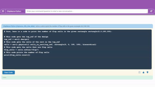
ChipNeMo in action. (Source – Nvidia)
Nvidia and the future of AI in chip development
The research paper essentially discusses the team’s endeavor to gather and utilize Nvidia’s design data to construct a specialized generative AI model. While initially focused on chip design, this process has implications far beyond, indicating its potential applicability across various industries.
The project began with a base model, further developed using Nvidia NeMo. The foundational model boasts 43 billion parameters, indicative of its pattern recognition capabilities, and was trained using over a trillion tokens, comprising words and symbols from texts and software.

ChipNeMo exemplifies how a specialized technical team can enhance a pre-existing model using their unique data. (Source – Nvidia)
Subsequent training phases involved around 24 billion tokens of Nvidia’s design data, followed by a mixture of approximately 130,000 examples of design conversations and layouts.


This pioneering work is among the early instances of research and proof-of-concept demonstrations of generative AI in the semiconductor industry, signaling the beginning of a new era in technological innovation and AI application. As this field continues to evolve, it’s clear that Nvidia’s contributions and explorations will not only reshape the landscape of chip design but also illustrate the vast, untapped potential of AI across diverse sectors.
READ MORE
- Next-gen CX is based on customer communication management systems.
- Enhancing Business Agility with SASE: Insights for CIOs in APAC
- 3 Steps to Successfully Automate Copilot for Microsoft 365 Implementation
- Trustworthy AI – the Promise of Enterprise-Friendly Generative Machine Learning with Dell and NVIDIA
- Strategies for Democratizing GenAI