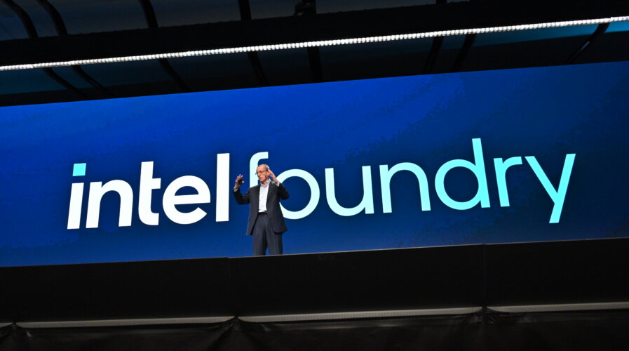
Pat Gelsinger, Intel CEO, introduces Intel Foundry during the Intel Foundry Direct Connect event on Wednesday, Feb. 21, 2024. (Credit: Intel Corporation).
Intel reinvents in semiconductor industry amid US$7 billion loss
- Intel and the semiconductor comeback: Overcoming a US$7 billion loss.
- Intel’s US$100 billion bet on future chip manufacturing dominance.
In recent years, Intel has embarked on a bold and transformative journey to reclaim its position as a leader in semiconductor technology. This ambition is embodied in the creation and expansion of its Foundry business division, a strategic pivot aimed at not only recapturing lost ground against rivals like Taiwan Semiconductor Manufacturing Company (TSMC) and Samsung Electronics but also establishing Intel as a pivotal player in the global chip manufacturing landscape.
Despite facing significant financial challenges, Intel’s leadership under CEO Patrick Gelsinger has laid out a comprehensive roadmap for resurgence and growth.
Intel’s strategic pivot in the semiconductor space
The operational challenges facing Intel’s Foundry business have been stark. In 2023, the division reported operating losses of US$7 billion, a notable increase from US$5.2 billion the year prior, alongside a 31% drop in revenue. These figures, reflective of the intense competition and rapid technological evolution in the semiconductor industry, have prompted a strategic reassessment at Intel, as noted by Reuters.

Amid these financial headwinds, Intel has undertaken significant structural and strategic shifts. One of the most critical moves has been the separation of manufacturing costs from the broader product development expenses on the income statement, creating a distinct category for Intel Foundry. This accounting realignment aims to provide a clearer picture of the foundry’s performance and the impact of production costs on Intel’s overall financial health.
At the heart of Intel’s strategy is a deep commitment to technological innovation and excellence. The company has announced ambitious plans to introduce five semiconductor process nodes over four years, a rapid pace of development aimed at leapfrogging competitors. A key focus is the advanced 18A technology, positioned as Intel’s counter to TSMC’s 3-nanometer node. With strong demand and several customer commitments already in place, the 18A technology represents a significant bet on Intel’s future in chip manufacturing.
Intel’s pivot to extreme ultraviolet (EUV) chip manufacturing technologies marks another critical aspect of its strategy. After initial hesitations that contributed to operational losses and competitive disadvantages, the adoption of EUV technology is expected to dramatically improve cost efficiency and product performance. This shift addresses past missteps and positions Intel favorably in the “post-EUV era,” as CEO Gelsinger highlighted.
Despite the current challenges, Intel’s outlook is optimistic. The company has outlined a path to break even by 2027, driven by efficiencies from EUV technology, reduced reliance on external contract manufacturers, and a growing portfolio of customer commitments. Intel’s ambitious investment of US$100 billion in expanding U.S. chip manufacturing facilities underscores its commitment to recovery and long-term dominance in the foundry space.
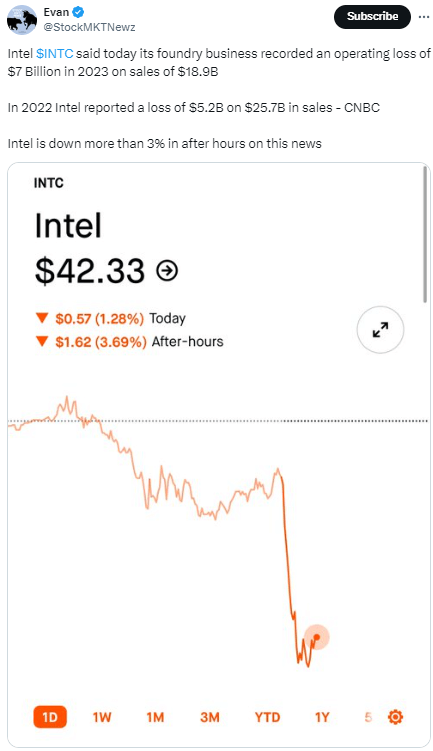
Intel’s US$7 billion loss spurs semiconductor industry reinvention (Source – X)
Expanding manufacturing footprint with federal support
Regarding this investment strategy, Reuters reported that Intel is embarking on an expansive effort to construct and enhance factories across four states in the U.S., buoyed by US$19.5 billion in federal grants and loans. Furthermore, the company is pursuing US$25 billion in tax incentives.
The focal point of this five-year initiative is to transform sprawling fields near Columbus, Ohio, into the world’s most significant AI chip production facility by as early as 2027, as explained by CEO Pat Gelsinger.
This influx of federal support comes courtesy of the CHIPS Act, underscoring the U.S. government’s commitment to revitalizing domestic semiconductor manufacturing.
Intel’s expansive blueprint includes upgrades to New Mexico and Oregon facilities and broadening its footprint in Arizona. This move comes as TSMC is also escalating its presence in Arizona, encouraged by President Joe Biden’s efforts to reinvigorate advanced semiconductor production in the U.S.
The financial aid from the Biden administration’s strategy to foster a semiconductor manufacturing renaissance is crucial for Intel’s recovery. Once a leader in producing the most advanced and compact semiconductors, the company saw its dominance wane in the 2010s as it fell behind TSMC, resulting in reduced profit margins from lowered prices to maintain market share with fewer products.
In 2021, Gelsinger unveiled a strategy to reinstate Intel’s position at the forefront of semiconductor manufacturing, acknowledging the need for governmental support to ensure profitability.
With this governmental backing secured, Intel is set to channel about 30% of its US$100 billion investment into construction, covering labor, piping, and concrete expenses. The remainder will finance the acquisition of chip-making equipment from companies like ASML, Tokyo Electron, Applied Materials, and KLA.
This equipment is pivotal for activating the Ohio site between 2027 and 2028, although Gelsinger cautioned that this timeline might extend if the semiconductor market faces downturns. Despite relying on grants and loans, Intel aims to fund most equipment purchases through its existing cash reserves.
Gelsinger has voiced that additional U.S. financial support for chip factories is essential for reasserting the country’s semiconductor manufacturing leadership, a sentiment he reiterated recently.
Despite federal support, Intel faces pressure to promptly demonstrate its competitiveness against Taiwanese and Korean rivals, according to Ben Bajarin, CEO of Creative Strategies.


Vision 2030: Intel’s Foundry ambition
The strategic realignment towards its Foundry business and aggressive technological advancements reflect Intel’s broader vision. By 2030, Intel aims to become the world’s second-largest foundry, boasting operating margins driven by innovation, cost-efficiency, and a robust client base. This vision is buoyed by the current lifetime value of contracts for the Foundry business, which stands at US$15 billion, and the anticipated benefits of transitioning to EUV manufacturing technologies.
Intel’s journey through financial turbulence and strategic shifts in its Foundry business division is a testament to its resilience and determination to regain its leadership in the semiconductor industry. Through technological innovation, strategic restructuring, and financial investment, Intel is not just aiming to navigate its current challenges but positioning itself for a future where it leads the next wave of semiconductor manufacturing.
As the industry continues to evolve rapidly, Intel’s efforts to redefine its operational and strategic paradigms will be closely watched by competitors and partners alike, marking a new chapter in the global semiconductor landscape.
READ MORE
- Safer Automation: How Sophic and Firmus Succeeded in Malaysia with MDEC’s Support
- Privilege granted, not gained: Intelligent authorization for enhanced infrastructure productivity
- Low-Code produces the Proof-of-Possibilities
- New Wearables Enable Staff to Work Faster and Safer
- Experts weigh in on Oracle’s departure from adland