
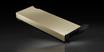
Nvidia achieves a breakthrough in chip manufacturing for ASML, TSMC, and Synopsys. (Photo by Mandel Ngan / AFP)
NVIDIA achieves a breakthrough in chip manufacturing for ASML, TSMC, and Synopsys
- NVIDIA unveiled cuLitho, a software library designed to accelerate computational lithography workloads, thus speeding up chip manufacturing processes.
- ASML, Synopsys, and TSMC will integrate NVIDIA’s GPUs and libraries into their software platforms and fabs.
- Soon, cuLitho will enable better design rules, higher density, higher yields, and AI-powered lithography.
The GTC developer conference by NVIDIA has just concluded, and amidst all the buzz on artificial intelligence (AI), the company unveiled that it has achieved a breakthrough in chip manufacturing. The advance is welcomed by semiconductor leaders, including ASML, TSMC, and Synopsys, as it brings accelerated computation to the field of computational lithography right as current processes reach the limits of physics.
The breakthrough brings accelerated computing to computational lithography using NVIDIA’s GPUs, enabling industry leaders mentioned above to accelerate the design and manufacturing of next-generation chips. Known as cuLitho, the new software library promises an exponential acceleration in chip design development times.
cuLitho also reduces chip fab data center carbon footprint and can push the boundaries of bleeding-edge semiconductor design. So far, NVIDIA cuLitho has already been adopted by the world’s top chip foundry, TSMC, leading EDA chip design tools company Synopsys, and chip manufacturing equipment maker ASML.
The idea behind the platform is to offload and parallelize the complex and computationally expensive process of generating photomasks used by lithography machines to etch nanoscale features, like transistors or wires, into silicon wafers.
“With lithography at the limits of physics, NVIDIA’s introduction of cuLitho and collaboration with our partners TSMC, ASML, and Synopsys allows fabs to increase throughput, reduce their carbon footprint, and set the foundation for 2nm and beyond,” Jensen Huang, founder and CEO of NVIDIA, said in his keynote address at the annual GTC developer conference.
How does NVIDIA cuLitho accelerate chip manufacturing?
For starters, it is necessary to understand how the cost of the computational time needed for the largest workloads in semi-manufacturing has, in recent years, been outpacing Moore’s law due to both the more significant number of transistors in newer nodes and more stringent accuracy requirements.
“Future nodes require more detailed calculations, not all of which can feasibly fit into the available computational bandwidth provided by the current platforms, slowing the pace of innovation in semiconductors. A fab process change often requires an OPC revision, creating bottlenecks,” NVIDIA said in a statement.
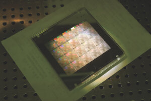
The new NVIDIA cuLitho software library for computational lithography.
Source: NVIDIA
That is when cuLitho comes in, and it will not only help to remove these bottlenecks but also make possible novel solutions and innovative techniques like curvilinear masks, high NA EUV lithography, and sub-atomic photoresist modeling needed for new technology nodes, NVIDIA noted.
Running on GPUs, or graphics processing units, cuLitho delivers a performance leap of up to 40x beyond current lithography — creating patterns on a silicon wafer — accelerating the massive computational workloads that currently consume tens of billions of CPU hours every year, NVIDIA noted.
It also enables 500 NVIDIA DGX H100 systems to achieve the work of 40,000 CPU systems, running all parts of the computational lithography process in parallel, helping reduce power needs and potential environmental impact. “In the near term, fabs using cuLitho could help produce each day 3-5x more photomasks — the templates for a chip’s design — using 9x less power than current configurations,” the AI giant said.
Essentially, a photomask that used to take two weeks can be processed overnight. Even more interesting is that cuLitho will enable better design rules, higher density, higher yields, and AI-powered lithography in the long term.
“Originally, photomasks were just a negative of the shape engineers were trying to etch into the silicon, but as transistors have gotten smaller, these photomasks became more complex to counteract the effects of optical distortion,” an article by The Register reads.
If unchecked, this distortion can blur these features beyond recognition. “This process is called optical proximity correction (OPC) and has more recently evolved into inverse lithography technology (ILT). In the case of the latter, the photomasks look nothing like the feature they’re designed to print,” the article stated.
That means the more ornate these photomasks get, the more computational horsepower is required to produce them. On the other hand, NVIDIA believes that using GPUs can speed up this process and reduce the power consumption needed.
“It’ll help the semiconductor industry continue the pace of innovation that we’ve all come to rely on, and it’ll improve the time to market for all kinds of chips in the future,” Vivek Singh, VP of NVIDIA’s advanced technology group, explained during a press conference on Monday.
Dashveenjit Kaur
| ![]() @DashveenjitK
@DashveenjitK
Dashveen writes for Tech Wire Asia and TechHQ, providing research-based commentary on the exciting world of technology in business. Previously, she reported on the ground of Malaysia's fast-paced political arena and stock market.
READ MORE
- Ethical AI: The renewed importance of safeguarding data and customer privacy in Generative AI applications
- How Japan balances AI-driven opportunities with cybersecurity needs
- Deploying SASE: Benchmarking your approach
- Insurance everywhere all at once: the digital transformation of the APAC insurance industry
- Google parent Alphabet eyes HubSpot: A potential acquisition shaping the future of CRM