- Lam Research says advanced packaging semiconductor Malaysia is the realistic near-term play.
- Memory shortages, panel-level packaging, and photonics reshaping what chipmakers need from the region.
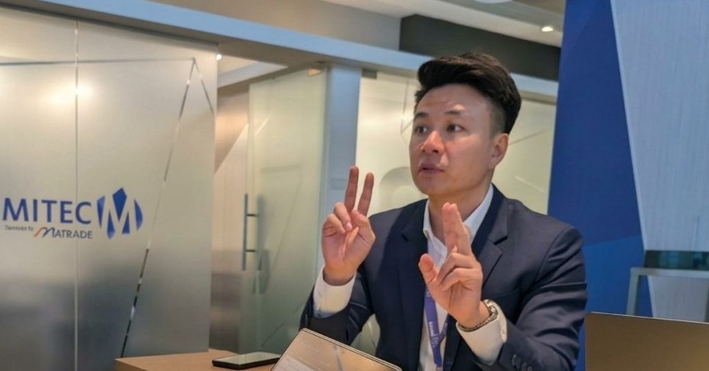
Malaysia keeps talking about the front end. The fabs, the wafer fabrication, the IC design – the high-capital, high-prestige work that Taiwan and South Korea have spent decades perfecting. But spend an hour with Andrew Goh, corporate vice president and general manager for Southeast Asia at Lam Research, and a different picture emerges: the real window for Malaysia in advanced packaging semiconductor development sits in the middle of the chip supply chain, and the country is running short of time to take it.
“Our ambition to be on the front end is a bit too for now,” Goh told Tech Wire Asia in an exclusive interview during SEMICON Southeast Asia 2026 at MITEC in Kuala Lumpur this week. “Today, if you look at Malaysia, we only have two fabs, doing very low legacy. They don’t even do advanced products.”
Global semiconductor sales hit US$795.6 billion in 2025, up 26.2% year-on-year, according to the World Semiconductor Trade Statistics. Equipment sales reached US$135.1 billion. The industry is growing fast but consolidating around a handful of players with decades of process expertise at the most advanced nodes.
Malaysia’s window to catch up on front-end manufacturing is, if not closed, extremely narrow.
The middle end, however, is a different conversation entirely.
The layer everyone is racing to master

Advanced packaging, the process of assembling multiple chips or chiplets into a single, high-performing unit, sits between front-end wafer fabrication and the traditional back-end assembly and testing that Malaysia has long been good at. Think of it as the connective tissue of modern chip design. And AI has made it more urgent than anyone anticipated.
Lee Chee Ping, managing director for marketing in advanced packaging at Lam Research, said: “The advanced packaging becoming more complex is really about integrating multiple chiplets, multiple suppliers, making sure technologically they can work well,” adding that the skill of collaboration is becoming more critical.
The reason goes back to physics. Moore’s Law, the observation that the number of transistors on a chip roughly doubles every two years, has been slowing down at the most advanced nodes for years. The industry’s answer has been to stop trying to cram everything onto one shrinking piece of silicon and instead stack, tile and integrate multiple specialised chips into a single package.
This is why the AI chips powering today’s data centres look more like a city block of interconnected components than a single processor. Lee used a more grounded analogy: imagine Kuala Lumpur. “I’m trying to make skyscrapers in the city. But at the same time, I need more people, more GDP, so I will [have to] expand the land of Kuala Lumpur.”
What Lee meant was that chips are not getting taller; they are getting wider. “Denser, but bigger as a system,” he added, noting that bidirectionality – simultaneously shrinking at the component level while growing at the system level – is what makes advanced packaging both technically difficult and commercially consequential.
Where Malaysia stands
Goh’s assessment of where Malaysia sits on advanced packaging was direct: roughly 10 out of 100, not zero. There is a base of assembly, test and some packaging ability in Penang and the Klang Valley, but nowhere near where the cutting-edge work is happening, which remains concentrated in Taiwan, South Korea and parts of the US.
“The complementarity between Malaysia and Singapore will be good to leapfrog the next advanced packaging area,” he said. “But it takes years for you to learn how to do a TSV properly.” TSVs – through-silicon vias – are the tiny vertical electrical connections that link stacked chips together, one of the foundational techniques in advanced packaging.
His prescription is to pick a specific niche in advanced packaging, and bring in the foreign investors who already operate in that space so local engineers can learn by doing.
“Identify the area, then you can invite foreign investment that has expertise in that area. That is the fastest way to get your people trained. Talent is how we started in Malaysia and Singapore; we bring in FDI, and people learn. So over ten decades or more, people learn how to do advanced packaging,” Goh said.
The FDI-led model that built Malaysia’s back-end ecosystem was always optimised for volume and cost, not knowledge transfer into higher-complexity processes. Changing that means being deliberate about which technology Malaysia wants to own and then structuring investment and talent pipelines around that specific bet, not the category at large.
The memory crunch
One thread running through the entire conversation is HBM (high-bandwidth memory), the specialised memory chips that AI accelerators need. Without HBM sitting beside the GPU, the whole system under-performs. Right now, the world does not have enough of it.
Lam’s own HBM-related tool revenue grew over 50% year-on-year in its most recent financial reporting.
But as TWA pushed Goh on, revenue growth does not automatically mean the right abilities are being built in the right places. His answer was candid – HBM remains the primary bottleneck, and the capacity constraint will persist because building a new fab shell takes 12 to 18 months minimum, with another year on top to commission equipment.

This crunch has also produced a strange side effect in the broader memory market. Because manufacturers are pulling resources toward HBM, conventional memory – the DDR4 and DDR5 chips that go into everything from laptops to industrial machinery – is now in its own supply squeeze. The old allocation system, where customers received a guaranteed percentage of supply, has broken down.
“In the past, there was allocation. But today, if I don’t have it, too bad,” said Goh. “They go to the outside market and buy.” A commodity that was once rationed is now a spot market. That has cascading effects in every device category that touches semiconductor components.
The next bet
On Lam’s own trajectory, Lee pointed to panel-level packaging as a major area of active investment. The concept involves processing chips on large rectangular panels, similar in principle to flat-panel display manufacturing, not the traditional round silicon wafers. A standard wafer today is 300mm in diameter; panel formats being explored run to 510mm or 600mm, which would dramatically increase the number of chips produced per processing run and open up new architectures for AI compute.
Lam made its entry into this space with the acquisition of Austrian wet-processing specialist SEMSYSCO in November 2022, gaining panel-level cleaning and plating abilities with an R&D facility in Europe.
“The product is already available in the market for R&D with customers,” Lee said. “But [customers] are very aggressively pushing for the final product.” The ecosystem around panel packaging – materials suppliers, substrate makers, inspection equipment – is still coming together, and Goh was honest that it involves a lot of smaller, non-traditional players stepping up. “The small players have to do it. Used to be LCD equipment guys, now they do the advanced chip.”
Photonics is the other technology, both flagged as the next shift. As AI workloads generate enormous amounts of data and heat, moving that data between chips and between servers using copper electrical signals becomes a bottleneck. Silicon photonics packages, which integrate conventional chips with optical components to move data using light instead of electricity, are being developed to address this.
“The push is towards photonics,” said Lee. “Communication between chip to chip, data centre to data centre, using cables will be costly and not energy efficient.”
The conversation Malaysia needs
The question surfacing at SEMICON SEA this week – from the exhibition floor to the panel sessions – is whether Malaysia’s National Semiconductor Strategy is specific-enough to translate into real ability. Goh’s view was measured: “First thing is to decide which area of advanced packaging you want to be in. Then you can invite foreign investment that has expertise in that area,” he said. Singapore, he noted, has been doing this longer: building R&D infrastructure and advanced packaging pilot lines that let engineers train on real equipment, creating the knowledge base that eventually lets homegrown players emerge.
Malaysia has the talent pool, the existing ecosystem, the infrastructure and the geopolitical neutrality that global chipmakers find appealing right now. What it needs is the specificity: not ‘advanced packaging’ as a category ambition, but a named technology, a named niche, and the industrial partners to match.
On whether Lam is part of the National Semiconductor Strategy discussions: “No,” said Goh. Make of that what you will.
Dashveenjit Kaur interviewed Andrew Goh and Lee Chee Ping of Lam Research at SEMICON Southeast Asia 2026 in Kuala Lumpur on 6 May 2026.

Want to learn more about AI and big data from industry leaders? Check out AI & Big Data Expo taking place in Amsterdam, California, and London. The comprehensive event is part of TechEx and is co-located with other leading technology events, click here for more information.
Tech Wire Asia is powered by TechForge Media. Explore other upcoming enterprise technology events and webinars here.